We meet Tuesday evenings 19:45 for 20:00, Thursday mornings 10:00 and Sundays 14:00. Tuesdays and Sundays are hybrid in person and Zoom meetings (Join us in person or using zoom, code 867 3049 5863) Thursday mornings are exclusively in person, see schedule below or contact us for more details.
Event Information:
-
A Simple Digital Power Meter
A Simple Digital Power Meter
by Dave Roberts, G8KBB
Ostermeyer Trophy Award Winner

Dave Roberts, G8KBB (left) and RSGB
President Don Beattie, G3OZF (right)In 1999 Dave Roberts, G8KBB, received the Ostermeyer Trophy as awarded by the UK Microwave Group for the "most meritorious description of a piece of home-constructed or electronic equipment published in RadCom."
Note: Some of the figures, circuit diagrams and images are small and may be difficult see on this web page. Click each image to open and view the image full size in a new window.
Introduction
One of the basic requirements we face is the measurement of RF power.
This article describes a simple to build, yet potentially accurate digital power meter. It is designed to operate as an inline power meter and displays the results on a 16 digit LCD display. It measures, in one range, power from 100 nW to 100W ( 9 orders of magnitude ) covering all HF bands up to 2 metres. It is usable with correction to 70 cms.
The meter comprises two separate parts, an RF unit and a display unit. The interface between them is a DC voltage across a specified range. It is therefore possible to reuse either part in different ways - for example the RF unit may be built without the digital display either to drive an exiting meter or as an RF sniffer.
The Specification
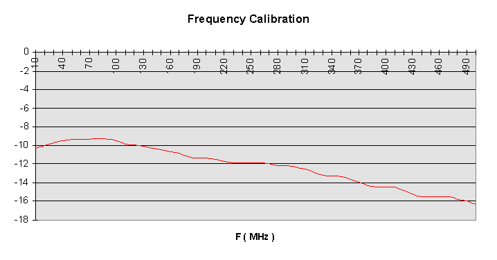
Figure 1 * The unit operates over a 90 dB range from 100KHz to 500 MHz and displays its results on the LCD display in both dBm and Watts. The power source is 9 to 15 V DC consuming about 12 mA. Subject to calibration - and that is a big assumption - the meter is accurate to within +/- 1dB from 200 kHz to about 175 MHz, and the deviation from log law is +/- 0.5 dB. The frequency response is shown in Figure 1, Figure 2 and Figure 3. At 70 cms it reads about 5dB low.
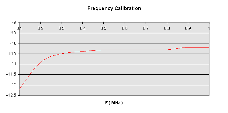
Figure 2 * The RF unit is based on the Analog Devices excellent log detector chip, the AD8307 [1]. The display is based on a single chip PIC processor, the PIC14C000 Mixed Mode Controller which requires programming. This can be achieved via a PC bi-directional parallel printer port using a small additional circuit if a programmer that will handle the 14000 is not available.
In the unit to be described, the range of the device is -40 dBm ( 100 nW ) to +50 dBm ( 100 W ) but the design can be easily modified for different ranges as will be detailed later.
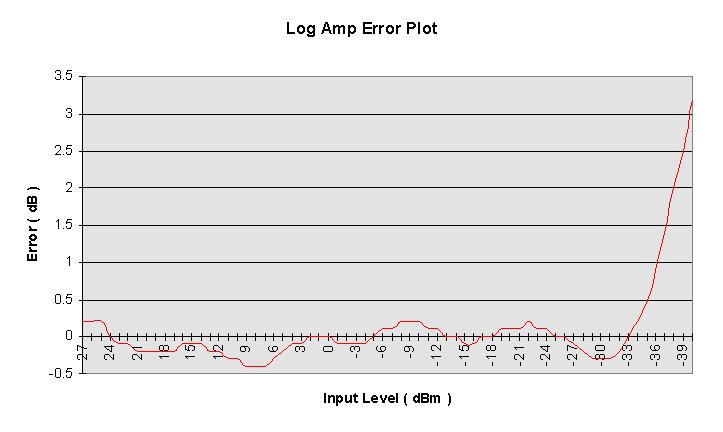
Figure 3 ** The digital display is not ideal for making adjustments to a circuit. If you wish to also use it for that, then put a small panel meter with suitable series resistor across the output of the RF unit. If you don't need the display just build the RF unit with an analogue meter. I may upgrade the software to add a simple bar meter and voltage display option at a later date.
Theory of Operation - RF unit
The RF unit is outlined in Figure 4, with the complete circuit shown in Figure 6. It is in reality a lie to call it a power meter. It is in fact a voltmeter, calibrated to give a DC voltage that corresponds to the RF voltage at its input. This is scaled to read in a calibrated manner when terminated in 50 ohms.
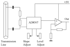
Figure 4 The RF voltage at the input is sensed at a BNC socket. Typically, this would be directly connected to a BNC T piece as the mismatch at the frequencies of interest here is not significant. The T piece is inserted into a correctly terminated coax transmission line that carries the signal to be measured. The voltage is AC coupled (hence the low frequency limit of the circuit) via a resistive attenuator into the AD8307 chip. This is described further below, but in essence it delivers a DC current corresponding to the RF input. This current is converted into a voltage by passing it through a terminating resistor and is then buffered and amplified to give the RF unit output voltage. With the values shown in Figure 5, the output voltage gives a range of 0 to 5 V with a 5V supply, giving 2.5V for 0 dBm input, changing by 0.5 V per 10dB change in input. The noise floor of the AD8307 gives a minimum signal of about 0.5V ( -40 dBm ) and the upper limit is 5V ( +50 dBm ). If you plan to use the digital display unit, then the value of R7 must be changed from 33K to 11K. This gives a range of 0V to 3V which matches the PIC processor ADC range. A reading of 0 dBm will then give 1.5V output, changing by 0.3V per 10dB input variation.
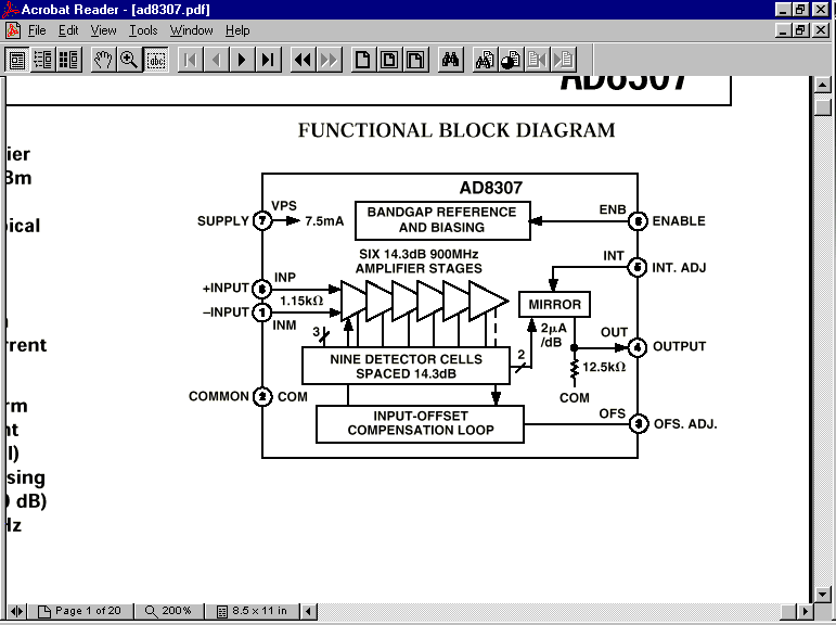
Figure 5
Reproduced from AD8307 Data SheetThe AD8307 is specified over the range DC to 500 MHz. A block diagram is reproduced from its datasheet [1] in Figure 5. The logamp has a 92 dB range to +-3 dB conformance and is +- 1dB over an 88 dB range. It is important to bear this in mind when using the unit. The display shows readings to 0.1 dB - but purely to aid seeing small relative differences - you cannot believe their absolute accuracy - that is at best +- 1dB. The INT and OFS inputs allow adjustment of the operation of the device. INT is designed to allow the intercept point to be adjusted - essentially an adjustment of the "no signal" output of the device. OFS is connected to the offset null circuits of the device. If you think about it, a DC coupled log amp operating down to microvolts will suffer from DC offsets in the amplifiers. To compensate for this, the chip includes an automatic offset null circuit that corrects continually for small errors. The OFS pin connects to the feedback loop within this circuit. In this application it is unused as its main purpose is to control the low frequency response of the device. Low frequency signals will tend to be cancelled by the offset null circuit. This is in part the reason for the low frequency tail off of the unit below 1 MHz. If it is desired to extend this low frequency response, a small ( e.g. 100 pF ) capacitor should be connected from OFS to ground. This will augment the on chip capacitor. The input coupling capacitors would likewise have to be increased. Keep the wires short if you do this.
The input signal is delivered to a differential input with a 1.15 K ( plus 1.4 pF ) load. The output voltage delivered is 25 mV per dB. This is achieved by delivering a current of 2 µA per dB into an internal load of 12.5 K.
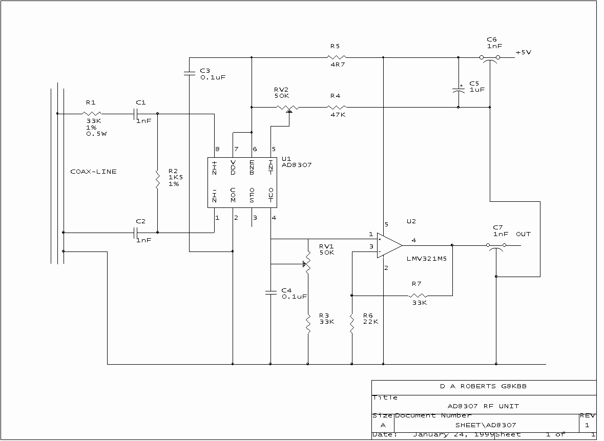
Figure 6 ***
RF Unit Circuit DiagramThe circuit shown in Figure 5 is a combination of two circuit suggestions in the manufacturer's datasheet. The basic method of operation as suggested by Analog Devices is a 1 kW power meter using an input attenuator resistor of 100 K. I found it difficult to achieve adequate performance with this impedance and am not interested in high power, so I settled for a 33 K input resistor and a 100 W range. If you wish to create a 1kW meter, change the resistor to 100K but you will need to be careful about construction. The PIC software allows it to be configured for full scale ranges of 1 kW, 100W, 10W or 1W. Incidentally, lower values of resistance, especially in R2, would improve frequency response. You might care to consider using values of 15K and 390R respectively. This would improve high frequency response at the risk of heating in R1 at high power levels. A 15K resistor would dissipate 1/3W at 100W assuming the line is properly terminated. If not, it could be much higher.
U2 is an output buffer formed of a rail to rail 5V op-amp. This is a surface mount fairly cheap device available from Farnell. If you do not fancy surface mount, then the board is easy to retrack for a DIL amplifier using a slightly larger box.
RV2 allows roughly 3 dB adjustment in the intercept point ( i.e. the absolute level of output to input ) and RV1 allows similar adjustment to the slope. This is achieved by altering the load resistor into which the current mirror delivers its signal.
The output lead from the op-amp should ideally be decoupled. If this is done through a standard 1 nF feed-through capacitor, then there is a chance that the op-amp may become unstable. The phase margin of the op-amp in the configuration shown with a 1 nF capacitor would be about 10 degrees, but feed-through capacitors are not the most accurate items in the world. They typically have a tolerance of -0% to +200 %. This means that a 1 nF capacitor may be 3 nF. Adequate stability at this level is not guaranteed. Therefore, you should use a feed-through decoupling capacitor of 100 pF or 470 pF if available. If not, use an insulated lead-through. If you do use a 1nF feed-through, and the op-amp is unstable, try a 1K resistor in parallel with the output which should increase phase margin by about 20 degrees.
How accurate is it really ?
Being honest, you will not see accuracy to within 1 dB. There are a number of reasons for this. Firstly, the AD8307 has its own inaccuracies. Secondly the unit is frequency sensitive. Thirdly the equipment against which it is calibrated will have an error and finally as it measures voltage not power non 50 ohm systems (for example VSWR not 1:1 ) will introduce errors.
Take an example. If the AD8307 is at the extreme of its specification ( 1 dB out ), the signal generator against which it was calibrated is out by 1.5 dB and you measure a signal on a line with a VSWR of 1.5 : 1 then the error could be as much as 4.2 dB.
In practice it will not be that far out, but exercise caution. The most significant place where care should be taken is in calibration. If you have a good oscilloscope, use it to check the signal generator level. If you have access to a second signal generator use it to check the first as well.
With care it will measure reasonably accurately but remember the display resolution is outrageously fine compared to the accuracy.
One final source of error. If the signal is modulated two things will happen. First the low pass filter in the AD8307 will show an asymmetry to the modulation due to the fact that it is charged from a current mirror and discharged by a resistor. Secondly and more significantly the ADC used in the PIC14000 will trigger early on the dips in the RF signal. This will cause the meter to read low. The signal is low pass filtered and effect is small but it is still noticeable. If this causes problems you might care to consider better filtering.
Construction of the RF unit
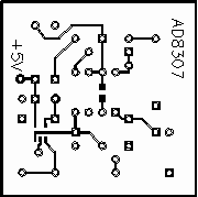
Figure 7
RF Unit PCB (bottom)The prototype unit was built into a standard 37mm x 37mm tinplate box. It comprises a double sided PCB used to provide a ground plane plus one signal layer, the artwork being shown in Figure 7 with the component placement in Figure 8 and Figure 9. The AD8307 and op-amp may be obtained from Farnell. The op-amp is cheap ( 35p ) the AD8307 expensive ( just over £10 ). The board is carefully cut down to size so that it will push fit into the box. The BNC connector is to be bolted to one end, so having cut the board to size, carefully drill the side of the tinplate box and bolt the connector to it. The board is fitted just below the socket so that the pin protrudes about 5 mm above the ground plane, but to achieve this it will probably be necessary to file a small recess into the edge of the PCB to allow for the rim of the socket.
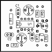
Figure 8
RF Unit Component Layout (top)When this has been done, drill the PCB. Don't forget to clear all non ground holes on the ground plane side so they will not short to earth, but be careful not to clear any holes that need to solder direct to the ground-plane - especially the AD8307 ground pin. Before soldering the PCB in though, don't forget to drill two holes one for DC supply one for output signal ) in the box in the face opposite the socket high above the ground plane and above the PCB connection pads. The power lead should be run through a 1 nF feed-through capacitor. The signal will be either through a feed-through or an insulated connector - see the text above.
The PCB may now be seam soldered to the tinplate box. When it has cooled, check that the lids can be fitted top and bottom of the box still. It is worth making sure that it is going to fit correctly before you solder it !
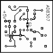
Figure 9
RF Unit Component Layout (bot)Now assemble the components on the top of the board. Leave the input attenuator resistor and trim pots until last. The AD8307 must not be mounted into a socket ( yes it is expensive but resist the urge ! ). The ground pin of the log amp plus all other earth connections solder direct to the surface of the ground plane. Turn the unit over and mount the two surface mount components. One is the AD8307 decoupling capacitor the other the op-amp. The decoupling capacitor is mounted directly between the power and earth pins of the AD8307. There is a simple way to mount SM devices. Use a cocktail stick to position the device. Cut a small piece of fine solder ( 1 to 2 mm long ) and place it next to the first pin to be soldered. Now hold the device steady with the cocktail stick whilst touching the tip of a fine soldering iron to the pad, solder and pin. The result should be a clean joint. Now solder the other pins similarly. The chip capacitor is an 0805 size device, the op amp an SOT23-5.
Finally, mount the input attenuator resistor between the pin of the BNC and the PCB. You may have to cut its length down to get it to fit. I also found it beneficial to put a small piece of copper foil around the resistor as a screen. A small L shaped piece is soldered to the sides of the box next to the socket and to the side and to the ground plane. Don.t get too fussy about this - just tack it into place with the iron but keep it clear of the BNC pin as far as possible.
Don't forget to connect the power and output signals.
Aligning the RF unit
The unit is designed to deliver a calibrated output covering 0 to 5V or 3V if it is to be used with the digital display. To achieve this, it is necessary to align the unit. There are two adjustments to make and the adjustment is largely iterative. In the following text, with the value of R7 set to 11K as detailed above, the voltages below will be different as shown below in parentheses.
RV2 adjusts the "level" of the input and RV1 adjusts the "slope". In order to align it, you will need an RF source at a known level of 0 dBm. This is best achieved from a signal generator and a stepped attenuator will also be needed. Connect a BNC T piece to the input socket, connect one side to the signal source through a stepped attenuator and the other side to a 50 ohm load. Connect a digital voltmeter to the output and apply 5V DC to the power pin. It should draw just under 10 mA. Check the calibration of the signal generator if at all possible.
What needs to happen next is simple, iterative and frustrating. You must adjust the two variable resistors for correct slope and zero point. First switch off the signal source but leave the dummy load connected. Adjust RV2 so that the DC voltage is about 0.45 V ( 0.3V for LCD display version ). Now apply 0 dBm and note the input voltage which should be roughly 2.5 volts ( or 1.5V ). Drop the input signal by 10 dB and the reading should drop by 0.5V ( 0.3 V ). Adjust RV1 slightly until it does. Now switch back to 0 dBm and adjust RV2 for 2.5V ( 1.5 V ). Repeat until you have a DC output of 2.5V ( 1.5V ) for 0 dBm input that changes by 1V ( 0.6 V ) for every 20dB change in signal level into the load.
Having achieved this, it is now worthwhile checking the linearity of the response over as wide a range as you have known signal for and check the accuracy across as much of the frequency range as you are interested in. Note that you can expect a small dip at high frequency as the AD8307, whilst good, is not perfect and the 1.5 pF input capacitance causes a roll-off. One thing to note in the non digital display version. The unit will deliver 5V for a full scale input from a rail to rail op-amp - but it needs a 5V supply. Give it 4.9 volts and it will top out at 2dB less than you were expecting. If necessary set the power supply slightly higher such as 5.25 V. With a full scale output of 3V for the LCD display version, this is not a problem.
You now have a working power meter that may either be used on its own or connected to the display unit. If you connect an aerial or similar pickup without a 50 ohm load, it also makes a neat RF sniffer or voltmeter.
The Digital Display
A block diagram of the digital display unit is shown in Figure 10 and the circuit is shown in Figure 11. The input voltage is scaled to a range of 0 to 3V to match the PIC ADC and fed into one of the PIC Analogue to Digital Converter ports. The ADC is capable of reading to between 8 and 16 bits resolution by timing the period needed to charge a capacitor to a given voltage from a stable current source. This is converted into an accurate voltage reading by performing trial conversions on a zero input and a known bandgap reference input. Note that the input must be driven by a low impedance source for correct operation. This is achieved by the op-amp in the RF unit. The 100K resistor connecting the input to ground is to stop it floating when disconnected, but the ADC of the PIC14C000 means that if disconnected the input will not sit at 0V but at a voltage slightly higher. Ground it and the display should show -50 dBm. For each displayed value, 8 samples are taken and the average is displayed.
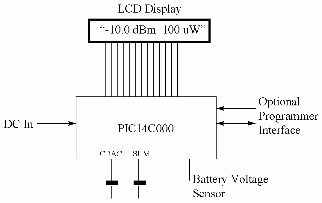
Figure 10 The software therefore derives a reading internally in volts in floating point format. This is converted to a notion of dBm by subtracting 1.5V and multiplying by a constant of 333.333. The result is an integer reading of dBm times 10 from -400 to +500 ( -40.0 to +50.0 dBm ). This is displayed on the LCD display. The reading is also converted into watts by performing a log table lookup and scaling the reading. It therefore displays power in dBm followed by Watts. The wattage reading is to two significant figures with decimal point or trailing zero as needed followed by the characters "nW", "uW", "mW" "W" or "kW".
The software is a crib from one of the Microchip application notes [2]. In this, a design for a battery monitor is given that measures voltage and current and sends the resulting readings serially as RS232 data. In this circuit, the RS232 module was removed and replaced by the power conversion and LCD display code. The bulk of the code is the original from Microchip.
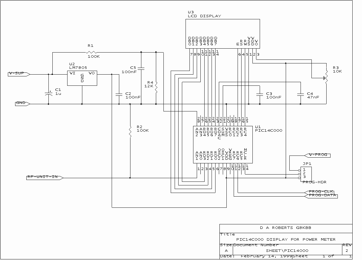
Figure 11 #
Display Unit Circuit DiagramThe software also performs two other functions. It measures the voltage on a second analogue input. This is designed to be connected to a resistive attenuator as shown in the full circuit diagram. This is scaled by the software so that when the input voltage falls below 8V DC, the power display will be replaced by "BATTERY LOW". In order to allow this feature to be switched off, the display reverts to power measurement if the voltage is below 2V. Hence it may be disabled by removing the resistor connected to the power supply.
Finally, the PIC processor needs to be able to time a ramp voltage created by a current source driving a capacitor. This is the capacitor connected to the CDAC input. When the program first starts to operate, it calibrates this slope. If it finds that it cannot because the value of the capacitor connected to CDAC is wrong, it will display "CDAC TOO LOW" or "CDAC TOO HIGH" as appropriate.
The detailed circuit comprises a 5V regulator, the PIC processor, a trimmer pot, five capacitors and three resistors ( and an LCD display of course ! ).
You cannot get a much simpler computer. There is not even a clock - the PIC does that internally itself which reduces RF emissions.
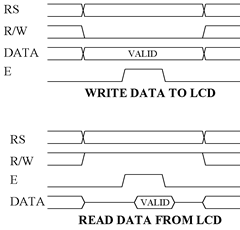
Figure 12
Timing Diagram for LCD ModuleThe LCD display is any of the alphanumeric displays containing the Hitachi HD44870 LCD controller family. These are available for about £12 from Farnell or Maplin but may also be picked up very cheaply from rallies or firms selling old stock lines. In general these have a 14 pin single in line or 20 pin dual in line connector pad block that is simply wired to the PIC PCB. The interface is an 8 bit data port, an enable signal, a Read/Write signal and a Register Select Signal. The communications used is shown in Figure 12. My second prototype used the Vikay 216 from Maplin.
Some displays such as the Vikay 216 split the 16 character line into two "logical" lines of 8 characters. To cater for this, the software will drive it as a two line display if the PIC OSC1 input is grounded.
The PIC processor operates from 5V, derived from a small 5V regulator. This also supplies power to the AD8307. Whilst the PIC is capable of regulating its own supply, I thought it better to provide a stable reference for the RF unit. You could use this with a MOSFET and eliminate the 5V regulator but it does not seems worthwhile.
No PCB is provided for the PIC processor. It is so simple it is easier to wire it up on a small piece of veroboard than to produce a PCB.
Programming the PIC
This is the only tricky bit. If you have access to a programmer that supports the PIC14C000 then the easiest way is to use that. If not, a simple interface circuit is provided as shown in Figure 13.
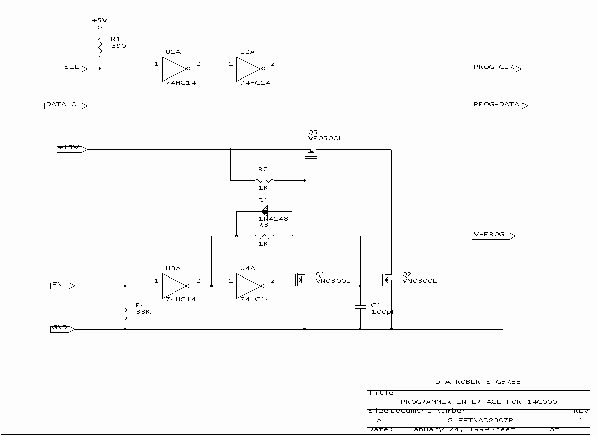
Figure 13 ##
PIC Programmer Circuit DiagramThe PIC is programmed by a serial interface consisting of clock and data. This is easily provided by a PC parallel port. In order however to read the data as well as to write it, this needs to be a bi-directional port for the circuit shown. Be a little careful here. If you have a really old PC, chances are it is the original IBM spec port that cannot read data on the 8 data lines. If it is more modern it may have a bi-directional mode or it may have the more recent EPP or ECP modes. These may often be switched into bi-directional mode by the BIOS. The data is written and read through bit 0 of the data bus on pin 2 of a DB25 LPT port. The select signal (pin 1 of the 25 pin parallel port connector) is used to clock the data. Pin 17 is used to switch the programming supply voltage. Pin 18 is one of many that can be used for ground. A short cable is constructed with a DB25 LPT connector at one end and connected to the display PCB via a small header.
Three simple DOS programs are available to program the device. These are CAL-14K, READ-14K and PROG-14K.
It is important that they be run from DOS and NOT from within Windows (that means reboot your PC into DOS and does NOT mean opening a DOS box from Windows).
Programming the PIC requires a series of 100 µsec programming instructions. In order to deliver this accurately, the CAL-14K program is used to calibrate a delay loop.
Programming also requires a 13V supply to the chip. Just to be awkward, the sequence of events needed for the PIC is as follows:
- Apply 5V to the PIC whilst holding MCLR low
- Whilst holding RC6 and RC7 low, raise MCLR to 13V in less than 8 µsec
- Apply sequence of load, increment, program and read instructions as required
- Drop MCLR to 0V ( fall time less than 8 µsec )
Full details are in the PIC14C000 programming guide [3] and datasheet [4]. The PROG-14K program takes care of the details.
In order to program the device, therefore, the circuit of Figure 13 may be added to the PIC circuit. This comprises a power MOSFET switch driven by a Schmidt inverter. It allows the PC to drive MCLR to ground or to 13V very quickly. Keep the wiring short as it will switch the voltage on and off in times less than 50 ns and 200 nsec respectively and ringing may occur. The programming circuit is connected to three signals from the PC parallel port.
Full details on how to use the software are not presented here. The PIC source code, object file, PC programs (source and executables) plus guidance notes are available on the internet. In overview though, the PC is connected by a short lead to the programmer board. The circuit is simple, and care must therefore be exercised in programming to avoid damage to the PIC. The CAL-14K program is run to determine the correct setting for a 100 µsec program cycle. This also has the side effect of ensuring that the signals from the PC are in a "safe" state. This is important. The PIC is plugged in and the jumper connected to MCLR is set to connect it to the programmer circuit. The power supply is set to a supply voltage of between 13 and 13.25 Volts and connected to the unit. The PROG-14K circuit is run to program the device. The supply is removed and the link reset so that, when it is next powered up, the MCLR pin is connected to the 5V supply.
Each PIC14C000 is programmed by the manufacturer with a set of calibration data that is specific to it. If you use a non windowed (and therefore non erasable) part then this is of little relevance. If you use an erasable device (the PIC14C000JW) then remember to read and save a copy of the device's specific values. These must be reloaded into the device after erasure. This is described in detail in the notes with the program. In all cases, the configuration data should not be programmed, and if you get this wrong you can prevent further programming of the device. The implication of this is that the watchdog timer will be active but the software caters for this.
Changing the program
There are two patch fields available which are not shown on the PIC circuit diagram. These are described in the software listings. One is used to select one of 4 different ranges. If you decide to use a different AD8307 input attenuator to achieve a different range for the meter, this field allows the range to be altered so that the maximum DC input corresponds to a display of +60 dBm ( 1 kW ) to +30 dBm ( 1W ) in 10 dB steps. The means to do this is shown in Table 4.
The second patch field allows reconfiguration to suit different LCD displays. A display may only have a single display line but logically it may be split into two lines. An example of such a display is the Vikay 216 from Maplin. With such a display, the first and second 8 characters are separate "lines". The PIC must therefore select two line mode and offset the data addresses by 40 for the second half of the line. This is configured by pulling the osc1 input low. For other displays such as the Hitachi 16 character modules this is not needed.
If you want to make a more radical change, then the PIC source is provided. This may be assembled using the Microchip assembler (current version is V02.20 available on free download from their website) and to debug the code requires MPLAB. This is also available free from Microchip website.
One such modification might be to make it into an RF voltmeter, and display not power but volts. This is something I may do in a software upgrade sometime.
Debugging the Display Unit
The display unit is simple enough to be easy to debug. The main problem is the connection of the PIC to the display. If when you power it up there is nothing shown on the display, and altering the LCD contrast trimmer R3 does nothing, connect a 'scope to RC5. You should find that this is normally low, and pulses quickly high after every set of readings (about 3 times a second). If you find it stuck at 1, getting set low temporarily every 2 and a half seconds, or simply low apart from a brief pulse every 2.5 seconds then it is likely that the PIC is failing to talk to the display properly and is being reset by the watchdog timer every 2.5 seconds. The way that it talks to the display controller is as follows.
During initialisation, it resets the controller. This is achieved by initially sending commands to the controller without waiting to see if the controller is ready, then once it believes that the controller is reset it sends commands and data by first checking the "ready" bit. This involves reading the ready flag from the controller by performing a control data read and checking data bit 7. Check to see if it is stuck at this stage (see Figure 12).
When performing normally RC5 is set low when the PIC is performing Analogue conversions and is set high when it is performing calculations and sending data to the LCD.
To check out the display range, you should find that it shows -50 dBm when AN1 is grounded.
Final Ramblings
You may find that having calibrated the RF unit, and connected it to the digital display it does not show quite the right result. To calibrate it, apply the RF unit and supply it with 0 dBm as before. It should read correctly. If not a slight tweak to the pots may be needed. I am afraid this is iterative. DO NOT get too hung up about the absolute accuracy of the unit. Don't forget that it is showing a display outrageously beyond its accuracy. It is at best accurate to 1 dB and will not be perfect across the frequency range.
Power supply is fairly easy to arrange. Anything that keeps the 5V regulator happy is fine - such as a PP3 or 12V supply. If your LCD display has an LED backlight though, be careful about how you supply it - or you will fry the regulator. Took me ages to realise what was making the horrible smell in my first prototype.
The tail off that can be seen in the frequency response is largely due to the input capacitance if about 1.5 pF interacting with the high values of input attenuator. Any additional strays introduced by the construction may make this worse. On the other hand it may make it better - but on the whole keep the wiring short & simple. In theory it would be possible to match out the capacitance by a much smaller value in parallel with the 33K resistor but this is very hard to do - the value needs to be about 0.2 pF. I had a try and gave up. Also note that if you change the input resistor to 100K you make the effects worse and if you lower it the effect is reduced slightly. The main determining factor is the 1.5K resistor. If you produce a better matching circuit for the range 0.1 to 500 MHz let me know. Finally it would be possible to compensate by getting the PIC to measure the input frequency and apply an offset automatically. The measurement only needs to be approximate but the complexity is not really justified. Maybe if the AD8307 gave an RF output from its log amp I would have done it - but a device with that much gain and an RF output would almost certainly be unstable.
Footnotes
* Plots of the displayed reading for a nominal input of -10 dBm.
** Note that figure 3 above is from an early prototype and low signal performance should be slightly better than this. The display shows the effect of the 14 dB cells in the AD8307. The kink near 10dBm is probably a measurement error.
*** See text in regard of the value of R7. It should be 11K if unit is used with digital display. Also see notes on output decoupling capacitor regarding stability.
# Note that pot connected to LCD controls contrast. For the Vikay display, connect it only to ground and the LCD - leave the connection to 5V open. In normal operation link JP1 pins 2 & 3. Omit R1 to disable low battery indicator. If display shows only first 8 characters, ground the osc1 input of the PIC. RC0 and RC1 control the display range.
## Note that SEL connects to pin 1 of DB-25 LPT port, DATA 0 connects to pin 2 of the DB-25, EN connects to pin 17 of the DB-25, Ground connects to pin 18 of the DB-25.References
[1] AD8307 Data Sheet, available from the Analog Devices website
[2] Microchip Application Note AN624, available from the Microchip website
[3] Microchip PIC14C000 programming guide, available from the Microchip website
[4] Microchip PIC14C000 Data Sheet, available from the Microchip websiteTable 1 - Parts List for RF Unit
Table 2 - Parts List for Display Unit
Table 3 - Parts List for PIC Programmer
PIC14000 Pins Range RC0, RC1 open circuit or pulled high 100W FSD RC0 grounded 10W FSD RC1 grounded 1W FSD RC0, RC1 both grounded 1000W FSD Table 4 - Meter Range Setting
Part Farnell Part No. Comments LMV321M5 101-590 SOT23-5 rail to rail op-amp PIC14000-04/SP 790-060 One time programmable PIC device (4 MHz) 28 pin 0.3" DIP PIC14000-04/JW 790-059 The more expensive erasable device (4 MHz) 28 pin 0.3" DIP AD8307AN 284-040 8 pin DIP log-amp Table 5 - Farnell part numbers for selected components
More
Links & References
Analog Devices Website Analog Devices Analog Devices AD8307 Information AD8307 Analog Devices AD8307 Data Sheet AD8307 Data Sheet Microchip Technology Inc. Website Microchip Microchip Application Note AN624 AN624 Microchip PIC14C000 Information PIC14C000 Microchip PIC14C000 Data Sheet PIC14C000 Data Sheet Downloads
Power Meter PIC Programs and Source Code pm_pic.zip Power Meter PIC Tools and Utilities pm_tools2.zip