


We meet Tuesday evenings 19:45 for 20:00, Thursday mornings 10:00 and Sundays 14:00. Tuesdays and Sundays are hybrid in person and Zoom meetings (Join us in person or using zoom, code 867 3049 5863) Thursday mornings are exclusively in person, see schedule below or contact us for more details.
Event Information:
-
A Headphones Splitter Box with Amplification
A Headphones Splitter Box with Amplification
by Ian White, M0BXR
Requirement
From time to time we require to run a rig for club events, these include demonstrations and open days, contests and expeditions. With all of these it is often necessary for more than one person to be involved in logging and checking and to be able to hear signals clearly sometimes in a crowded environment with other people talking.
The headphone socket fitted to many rigs is fine for a single operator in the shack and gives a choice of one pair of phones or a speaker.
In the group situation we often want more than one pair of phones for an operator and logger and the speaker as well so everyone else can hear. Often people bring along phones of different types mono / stereo high or low impedance.
Solution
In order to fulfill this requirement it was decided to investigate ways of splitting the headphone signal whilst preventing the muting of the speaker.
This can be simply achieved by taking audio from the rig at around line level after the detector stage but before the volume control and audio output stage. In effect we are adding a completely separate audio channel to power the headphones whilst leaving the original signal untouched to still pass through the internal tone and volume control and be amplified to give speaker output.
Scope
The details of the project are widened to include information about using a free PCB design program to make a board layout and a photographic process to prepare and etch the circuit boards. This process is not new to the club but by including details here it is hoped to give members the details they require to build simple single sided circuit boards.
Circuit Description and Components
The design allows up to four pairs of headphones to be attached to a rig. The signal is taken from the rig by a single audio lead and goes through a volume and tone control network. The volume control is 100k which is fairly high impedance so that it does not load the line output of the rig. Rigs like the ICOM 756 Pro have an ouput impedance of about 10K so we would not want to go below this level.
 After the volume control the signal passes to a TBA820M IC which can provide 2 watts of output into an 8 ohm load, in actual fact the power required by headphones is only a few mW but in the interest of connecting headphones of different types the extra power available allows more flexibility.
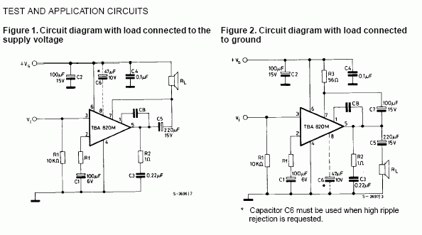 The tone control used in this design is a simple treble cut control which will help reduce certain types of noise and make the audio less shrill, there are other ways in which the audio could be improved eg. by having an active filter of variable width and centre frequency to tailor the response between 200 an 4Khz. Another possibility is that a DSP board could be fitted. For this reason and also so that an isolation circuit for digital modes can be fitted I have used a larger box than necessary for the amplifier boards.
Each box has two identical PCB's in it each with their own volume and tone controls to so they can be set to suit different users.
The TBA820M has an op amp type differential input and requires only a few external components.
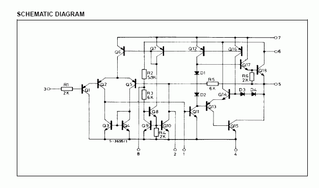 The circuit adopted is fairly consistant with the ground connected load above. Some component values have been rounded to make use of available parts. Below is the internal structure of the IC which has an op amp voltage amplification stage followed by an output current amplifier using complemntary transistors in a Darlington arrangement. Other components control the biasing and current stability which is an inherant part of the design. Another similar IC which was considered was the LM380 and in fact the PCB layout does include some extra tracks so that an LM380 could be used as an alternative however this has not been tested.
Making The Circuit Boards
The techniques here are not new but are a useful method for making small quantities of circuit boards for amateur radio and other electronic projects. The circuit board to be described is quite simple and only single sided, the technology can be extended to produce double sided boards. The program used will also create 4 layer boards however these will require a specialist company to manufacture them such as the company that supplies the program Express PCB. This is a free program which can be downloaded from several sources, it is easy to use with possibly the exception of printing but I shall describe a way of printing on transparant film which is required to complete the process.
Download and information about the program is available at Express PCB.
For printing Irfan View is recommended and can be downloaded from IrfanView.
For a simple single sided board auto layout is not required so you do not need to use the companion program expresssch.
The program is downloaded and installed like any windows program, if setup does not run in XP the program can be installed in safe mode.
On starting the program a grid will appear. The default spacing is 0.1" and the first step is to adjust the work area to the size of your board.
Next use the component manager to place the larger components on the work area paying particular attention to positioning of sockets and controls. ICs should be placed with a reasonable space around them for smaller components. The layout can be achieved by simply tranposing the circuit into track layout, use horizontal and vertical lines wherever possible for clarity and use thicker track for ground and supply, it is easier to lay out the circuit this way and also gives less resistance where more current flows.
The layout should all be on one side of the board and the screen view is from the top so that IC pin outs will increment clockwise around the device. The silk screen layer was not used with this simple board.
The program is easy to use and help files can be followed so the only further details about using the program regard printing. In order to use light sensitive board we require a transparency printed the same size as the final board and with all the copper areas black, the centres of pads are clear. You will find that using the print option from this program always prints with a grey area and the grid is also displayed, This happens even when the display on screen is black and white. Unfortunately this is not suitable for our purpose. There is an easy workaround this problem.
When the layout is complete set up the colours [View|Options|Colours] so that the background is white and the copper layer is black, any other details you do not need should be set to white and text in layers you need should be black. On the screen you now have in black the copper area that will remain on the board note its as viewed from the top of the board if it were transparent.
At this point press the Print Scrn key and then open Irfanview and paste in the image. Use the crop feature of Irfan View to remove unwanted peripheral areas of the screen. Print first to A4 paper and check the size of the image against the components. Irfan view is cabable of printing any size. Use the print dialoque box to print the circuit to its exact size. Finally when the correct settings have been established print it onto clear film. Two copies will normally be required.
Using The Light Box To Expose Light Sensitive Board
The light box is a simple device and consists of a wooden box with a hinged lid the inside of which has a foam layer. Inside the lid is a glass pane on which is placed the transparent image and the circuit board.
 On closing the lid the circuit board and transparency are held in contact so that a fluorescent tube in the base of the box can expose the areas where copper will be removed to light.
The light should have warmed up before the circuit is placed for development and should be left in for a specific time usually around ten minuites.
The time will vary with different batches of board and chemicals and small test pieces may be used to get the conditions right by trial and error.
Using Chemicals To Develop The Board
The process used to develop the board requires three raw materials, these are all readily available from electronics stockists such as Maplin, RS or Farnell in the UK and doubtless other countries will have there own suppliers.
Firstly photosensitive board is required. This is available in different qualities and sizes. CPC's part number PC00032 was used but other sources, sizes etc, are just as good. The board can be cut to size by scoring on both sides with a Stanley knife and then applying pressure to break along the cut line. The board is supplied with a black protective film on the photosensitive side and this should only be removed when the board is placed in the light box.
After exposure to UV light for about ten minutes the coating emulsion is removed from the exposed areas using caustic soda or sodium silicate.
 A word of caution here caustic soda is a strong alkali which will certainly degrease your skin and burn if concentrated, spillages should be washed away with water or vinegar. Goggles are advised when using to avoid eye contact. The strength of solution used for the process is quite weak however and is made by dissolving a level teaspoonful of solid caustic in a tumbler (500ml) of water. The solid product can be bought from a hardware shop and is used for cleaning drains.
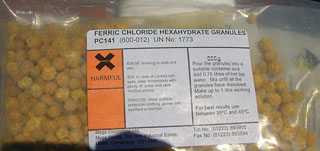 Caustic Soda illustrated on the right and below right ferric chloride which is used to etch the board after the emulsion has been developed with the caustic. Ferric chloride is also and unpleasant and corrosive chemical which when added to water contains free hydrochloric acid. Spillage can be treated by adding a weak alkali such as sodium carbonate ie washing soda crystals.
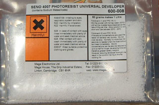 Follow the manufacturers instructions illustrated above to make up ferric chloride solution. Sodium silicate is a safer but more expensive alternative to caustic soda, image below.
When using the chemicals prepare just sufficient for immediate use and ensure containers are clearly labelled.
Dark room trays can be used to place the circuit boards in for development and etching. Polythene sandwich boxes and many margarine containers are also suitable but avoid containers made from aluminium and other metals which will most certainly be affected by one or both of the solutions. Special baths may be purchased which pump etchant around the boards.
The Process
Once you have all your solutions and containers to hand and have printed out your film this is the process to follow. Do not expose the photosensitive board to light more than is necessary, however a dark room is not required providing you work quickly and methodically.
1. Switch on your lampbox and allow it to warm up for 5 mins.
2. Place your film in the lightbox with the top uppermost ie the black area is the way you would see it if looking through the board from the top.
3. If an inkjet printer is used align two layers of the image so they match exactly and hold together at an edge with masking tape. This is because most inkjet printers do not produce an image which is solid and dark enough to give good results. If you are using a laser printer you will normally not need to do this.
4. Place your cut piece of circuit board over the film taking care that it is correctly positioned with the circuit. use a pen to mark the edge if necessary. Just prior to final placement the black film is removed from the board and this side faces down towards the light.
5. Time the exposure using a stopwatch or kitchen timer.
 6. After the alloted time usually around ten minutes place the board in to a tray containing the alkaline developer. Times vary greatly here but can be as little as 20 seconds, what you should see is the emulsion layer darken to a blue black colour and fragment where the light has reacted with it. When this occurs wash the board under the tap some gentle rubbing after the caustic has rinsed may aid the removal of the emulsion if it has not fully developed but abrasives should be avoided. If the emulsion is stubborn leave it a bit longer next time. If the track pattern washes off as well repeat using a shorter time in the light box ie two minutes less and shorter time in the caustic also until a good image is acheived. Use small offcuts of board if necessary to get your timings right. The board should now look something like this.
7. Etch away unwanted copper by placing in ferric chloride solution. Agitating the tray will keep the solution moving and speed up the process. Also the solution can be warmed before use.
Eventually you will have a circuit board with the copper pattern on it and no copper between the tracks. Rinse and dry.
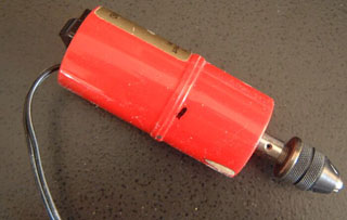 The board can now be drilled with a small 12 volt drill. The drill can be hand held providing reasonable care is taken. Most of the holes are 0.8mm but a slightly larger bit can be used for the jack sockets.
8. Complete the board by inserting and soldering the components using a temperature control iron.
Testing
Check all the components are correctly placed according to the circuit diagram, note that the layout used has some spare track and holes which were incorporated so that an LM380 could be used.
If all is correct apply an input of about 300 mv from a signal source, plug in headphones and apply power. On turning up the volume the signal should be heard.
 Finally the case can be drilled for the sockets controls and cables and screwed together as required.
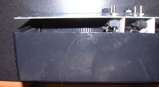
The box used in the prototype measured 17.8 x 10.8 x5.9 mm internally had has slots to keep the circuit boards in place. The jacks and controls are joined to the lid with nuts.
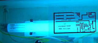
The photo below shows the alignment of the boards etc as the lid goes on the box.
Disclaimer:
Warrington Amateur Radio club, this website and its authors will not be held responsible for damage or injury caused by the misuse of any chemicals. Always check the manufacturers instructions and safety recommendations when using chemicals.