


The CDG2000 Front End Board
This is an old version of the article submitted to RadCom. It contains some additional material not published. The pictures, artwork and layout data on this page are of reduced quality. High quality downloads are available from the front end board main page. Note that the pcb, schematics and component list are not in this document, please refer to the main page for the front end board.
Return to Front End Board page
The CDG2000 High Performance Transceiver (Part 2)
The Front End Board
The front end comprises the following main blocks
- Relay switching for TX/RX & attenuators
- A 9 MHz notch filter
- A set of band pass filters
- An H Mode mixer
- An SSB bandwidth roofing filter
- A computer control interface
A block diagram is shown in Figure 1.
The board is controlled by means of a two wire I2C bus. The controller may change the TX/RX switching, attenuator and bandpass filters. This interface is optional, it may be replaced by a parallel interface by omitting the I2C bus interface chips and connecting a logic level signal to the relay drivers or by also omitting the relay drivers and driving the relays directly.
The attenuator provides two switchable attenuators of 6 and 12 dB, allowing 0 to 18 dB of attenuation in 6 dB steps. The 9 bandpass filters are one per band. In each case the band filters cover a complete band, there being no separate 500 kHz filters for 10m where a single filter covers the band. A notch filter reduces IF breakthrough.
The local oscillator from the synthesizer is divided by 2 in order to provide two signals 180 degrees out of phase for the H mode mixer.
The mixer is bi-directional, accepting either a 9 MHz transmit input and generating a transmit signal or generating a 9 MHz IF from an incoming RF signal.
The receive signal is passed through a 9 MHz roofing filter before being output to the IF.
A photograph of the top of a prototype board is shown in Picture 1 and the track side in Picture 2.
Detailed Circuit
The full circuit diagram is shown in Figure 9 and Figure 10, and each of the main blocks, as defined above, are detailed below.
Attenuator
The attenuators are simple resistive pads. Each presents 50 ohms input & output. The relays are controlled by the controller via the I2C bus. The main point to note, as is the case with all relays on the front end, is that the contacts carry a DC wetting current. This is to ensure that they do not develop poor (in other words noisy) contacts in use.
Notch Filter
The performance of the notch filter is shown in Figure 2. This is by measurement not calculation. Its purpose in life is to prevent large signals on the IF frequency of 9 MHz getting through to the IF.
The green line shows the reference signal and the red the loss through the notch filter. As can be seen, it presents a loss of over 40 dB at the desired frequency and its loss is negligible on any of the amateur bands with the exception of 10 MHz where it incurs a loss of 1.5 dB. This is the band where it is most needed as the desired signals are but 1 MHz away from the IF.
The overall performance in terms of IF rejection is a combination of the notch, bandpass and RF port isolation loss of the mixer.
Band Pass Filters
There is one band pass filter per Amateur band. The filters are 3 section Butterworth designs with a loaded Q of about 8. It varies a little by band. The 50 ohm design impedance’s determine the coefficient capacitors ( the ones to ground ), and the series LC circuits define the bandwidth and resonant frequency. The values chosen were based on Toko ready wound components. The basic design is the same as for the crystal filters shown in the RSGB Handbook [7] and the performance of each is tailored to the band in question with losses that vary slightly by band as shown in Table 1. You will notice some significant variation in the readings for IP3. This is because two different types of coil were used in its construction. The 21 and 24 MHz filters used Lodestone Pacific L45-6 formers, the rest used pre-constructed Toko coils. It was found that the performance of the receiver was different using Lodestone and Toko coils in the band pass filters. When using pre-wound coils from the Toko range, the IP3 performance varied between different types whereas when using hand wound coils on Lodestone formers, performance was more consistent. The variation in performance was up to 15 dB as can be seen from Table 2. It is presumed that this is due to saturation in the cores but opinion varies. The Lodestone formers have the same pinout as the Toko and fit the same PCB but the cases are marginally larger with substantial ferrite content. If the difference is that dramatic why show the Toko data?. Not everyone will want to be bothered winding coils and not all were poor. The board takes both types of coil and the constructor can decide which to use. The components list shows both Toko and hand wound Lodestone inductors.
Performance plots of all the filters is available from the web [1]. Examples are shown below in Figure 3 and Figure 4 of the 7 MHz filter. Note the effect of the 9 MHz trap. The wideband performance plot is limited by the analyser used in the measurement not by the filter.
The insertion loss when all relays were off was measured. It was found that the loss was acceptably small to 20 MHz but from there rose significantly to be only 30 dB at 200 MHz. To improve this, the relays were decoupled and inductors fitted in series with each relay control line. This reduced the signals at 200 MHz by over 40 dB. Specifically, the relay coils on the aerial side were decoupled with 10 nF capacitors, the mixer side relays by 1nF and the series inductors between the relay coils were 0.82 uH, self resonant at 200 MHz. Additional connections from the earth tracks between the relays to the ground plane were made in 3 places on each side. These structures can be seen on the photograph of the board. The 12V line was also decoupled and filtered in the same way.
The Mixer
The mixer has already been well described before in both Technical Topics [3] and in the RSGB Handbook [4]. It is capable of excellent performance both in regards of IP3 and insertion loss. The VCO is applied to U1, a high speed JK flop flip which produces two signals 180 degrees out of phase at the desired local oscillator frequency. These are then fed to the mixer. The mixer is formed by 3 identical transformers and a high speed bus switch. Note that the supply to the mixer is not 5V but 7V, derived from a 317 type regulator whilst the flip flop is driven at 5V. Both supplies are well filtered. The input signal from the local oscillator is a CMOS level signal and may be applied directly to the JK Flip Flop but the board is designed to allow other oscillators to be used and a signal between 0 and 10 dBm may be used.
The JK Flip Flop used may be either the 74AC112 or 74AC109 according to availability but slight adjustment of the PCB tracking will be needed for the 74AC112.
The insertion loss of the mixer has been measured at between 4 dB at 30 MHz and 5.5 dB at 2 MHz. Its input IP3 is 37 dB at 14 MHz and 40 dB at 3.5 MHz. This is below the levels first reported for this configuration [3] and is believed to be due to changes in the manufacture of the transformers. It has however been measured consistently.
Isolation across the mixer has been measured as between 45 and 65 dB from RF to IF port.
Roofing Filter
The roofing filters job is to protect the post mixer amplifier from large signals. It must also possess a large IP3 itself and present an acceptable load to the mixer. The filter actually comprises the following parts:
- A diplexer to present 50 ohms at frequencies removed from the 9 MHz IF,
- A hybrid coupler to drive 2 bandpass filters,
- The 2 bandpass filters,
- A hybrid combiner at the output of the filters.
Why the complexity? The use of this type of a structure has been described many times before for example in RadCom [5]. The main reason is that a filter on its own will be nowhere near its design impedance outside its passband. Combining two identical filters however allows the errors to be cancelled leaving a much more stable impedance.
In our design, each of the two bandpass filters is constructed from 4 ladder networks of identical 9 MHz crystals. The performance of these can be seen in Figure 5. The two curves show the measured performance of the two filters. The overall performance of the two filters and the diplexer / hybrid is shown in Figure 6. The insertion loss is about 2 dB for the filters, diplexer and hybrids combined.
The performance of each filter is not quite identical, resulting in a slight mismatch. No plot of return loss is available. As an alternative to discrete crystals, a PCB that takes standard commercial filters is also available.
When using discrete components in the roofing filter, care is needed. The filter is narrow and must be on the same frequency as the main crystal filters on the post mixer amplifier board. If you wish to use commercial filters, we suggest you consider International Radio Corporation [2]. Further information can also be found on the Warrington ARC web site [1].
Construction
The Front end board is, unlike the other CDG2000 modules, not a single Eurocard. This is because the filters would not all fit on one and it made no sense to artificially divide the circuit up into blocks. The board is 228 x 140mm. It is single sided with a ground plane and a small number of wire links. The mixer active device, a CMOS bus switch, is surface mounted on the rear of the board. Many decoupling capacitors and the inductors isolating the two sets of band switch relays are also surface mounted. Picture 1 shows the top of the board, Picture 2 shows the bottom of the board, Figure 8 shows the top component placement, Figure 7 shows the tracking of the PCB. Table 4 shows the components list. All artwork is available online from [1].
Note that all grounds are soldered direct to the ground plane. Use turned pin sockets for all DIP ICs, the ground pins of which can easily be soldered directly to the ground plane.
In construction, start with any part of the circuit you like, but it makes life easier to build the roofing filter before the mixer and don’t insert the coupling capacitor from bandpass filter relays to mixer input until all parts are working.
Having built the roofing filters, you need to check that each is working correctly. The filters should be checked individually by removing the input connection to the hybrid for each filter in turn, replacing the filter input by a resistor. Each should be of similar performance see Figure 5. Now connect both and the performance should be as in Figure 6. If you have access to the necessary test equipment, the return loss of the whole configuration should be low. If not, connect a 50 ohm signal source such as a signal generator and monitor the input with a x10 scope probe. The voltage presented by the signal generator should be constant across a wide frequency range and show no large discontinuities near the 9 MHz design frequency. The loss of the whole diplexer / hybrid / filter / hybrid assembly should be about 2 dB and the 3 dB bandwidth should be about 2.4 kHz as shown in Figure 6.
For the mixer, it is suggested that you check the voltages provided by the regulators before you fit the active devices. The 7V rail may need a tweak to the resistors. Now fit the divide by 2 and use a scope to check its operation. It should work correctly to beyond 80 MHz with a signal of between 0 and 10 dBm.
The mixer may be tested by applying a signal to the local oscillator and a second signal to the mixer input, with a 9 MHz expected output that should be visible with a scope or spectrum analyser at the roofing filter output.
The notch filter should be tested before connection to the bandpass filters. Tune for maximum attenuation at 9 MHz.
The bandpass filters should be tested one by one. The best way to align them is with a spectrum analyser and tracking generator. Failing this, tune all 3 for best signal at band centre then tweak slightly the outer 2 coils for best shape.
Performance
Many aspects of the performance of the front end have been presented in the preceding text. What can be expected of the whole unit?
The IP3 of the bandpass filters varies from +30 to +45 dBm according to the type of inductors used. At the upper end of bandpass filter performance, it is dominated by the input IP3 of the mixer of +37 to +40 dBm. Assuming a 2 to 3 dB bandpass filter loss this gives an equivalent IP3 for the mixer at the input of the filter of +39 to +43 dBm. If the bandpass IP3 is 43 dBm, the overall IP3 is +37 to +40 dBm ( roughly ). For lower bandpass filter IP3, the performance of the filters will dominate. For higher performance, the mixer dominates.
Note that mixer IMD was measured in conjunction with the roofing filters, and was not noticeably degraded for close in signals of a few kHz spacing.
The roofing filter works well for SSB signals in protecting the subsequent circuits, but close in ( i.e. for CW) IP3 will be degraded slightly if the post mixer amplifier has inadequate performance. However, at these spacings, the chance of the received transmission being clean enough for the receivers performance to dominate is very small indeed.
Overall noise performance was determined by measuring the 10 dB SNR of the receiver using the test setup to be described later, in the synthesizer article. On SSB it was found to be 120 dBm +/- 1 dB across all bands as shown in Table 3. The method used was to connect a PC sound cards microphone input to the output of the receive product detector and use DL4YHFs Spectrum Lab program [6] to determine SNR. The program displays the spectral analysis of the audio signal, for example as shown in Picture 3. It is then instructed to calculate the largest signal in the range 1000 to 2000 Hz and subtract from it the calculated per Hz noise power and a correction of 34 dB to account for the bandwidth of the SSB filter by executing the program
print(peak_a(1000,2000)-34-noise_n(1000,2000))
and to repeat this calculation every second. This causes it to directly display Signal to Noise ratio once a second. Note that this is S/N not (S+N)/N.
Interestingly, a small improvement is possible by removing the 50 ohm resistor in the roofing filter output hybrid. Is this due to resistor generated noise reflected back from the bandpass filters?
References
- http://www.warc.org.uk/
- http://www.qth.org/inrad/
- Technical Topics RadCom September 1998 p58
- RSGB Radio Communication Handbook, 6th Edition, pp 6.48 to 6.53
- RX84, Rad Com, May 1994 pp13-16
- DL4YHF spectrum lab program http://www.qsl.net/dl4yhf
- RSGB Radio Communications Handbook, 6th Edition, Figure 6.46 p 6.26
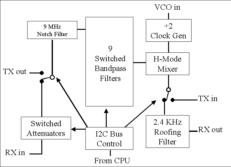
Figure 1 – Front End Block Diagram
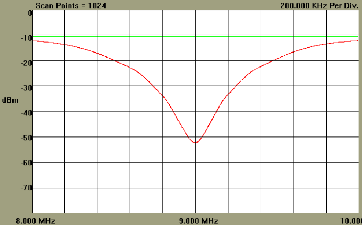
Figure 2 – Notch Filter Plot
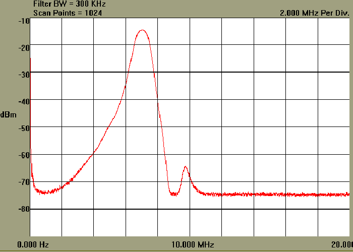
Figure 3 – 7 MHz filter
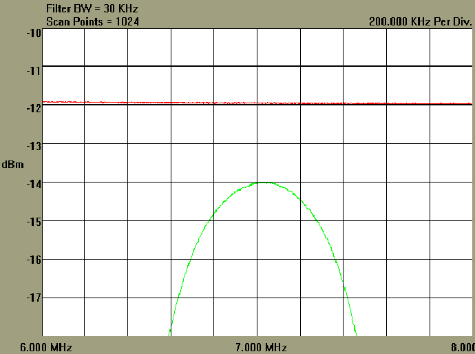
Figure 4 – 7 MHz filter
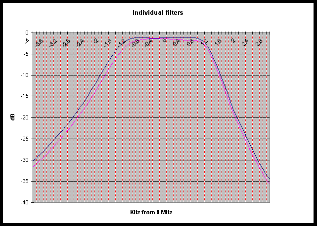
Figure 5 – Roofing Filters
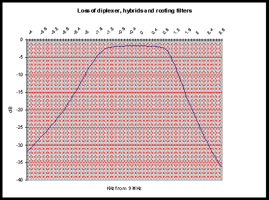
Figure 6 – overall roofing filter shape
|
Band |
Loss (dB) at band centre |
Loss at band edges ( dB ) relative to band centre |
IP3 ( dBm ) |
||
|
Low |
High |
Output |
Input |
||
| 1.8 � 2.0 | 2 | -0.5 | -0.75 | 33 | 35 |
| 3.5 � 3.8 | 1.5 | < -0.25 | < -0.25 | 37.3 | 38.8 |
| 7 � 7.1 | 2 | 0 | < 0.25 | 31.5 | 33.5 |
| 10.1 � 10.15 | 3 | 0 | 0 | 26.7 | 29.7 |
| 14 � 14.35 | 2 | 0 | 0 | 42 | 45 |
| 18.068 � 18.168 | 3 | 0 | 0 | 32 | 35 |
| 21 � 21.45 | 2.8 | 0 | 0 | 40 | 42.8 |
| 24.8 � 25 | 2.5 | 0 | 0 | 40 | 42.5 |
| 28 � 30 | 2 | -1 | -1 | 34.5 | 36.5 |
Table 1 – band perfomance
|
Band |
Loss (dB) at band centre |
Loss at band edges ( dB ) relative to band centre |
IP3 ( dBm ) |
||
| 21 � 21.45 | 4 | 0 | 0 | 25 | 29 |
Table 2 – performance with Toko coils
|
Frequency |
Level for 10dB SNR |
| 1.90252 | -121 dBm |
| 3.73202 | -121 dBm |
| 7.02929 | -121 dBm |
| 10.14888 | -120 dBm |
| 14.31673 | -120 dBm |
| 18.13473 | -120 dBm |
| 21.29647 | -119 dBm |
| 24.87047 | -120 dBm |
| 28.35293 | -119 dBm |
Table 3 – 10 dB SNR measurements
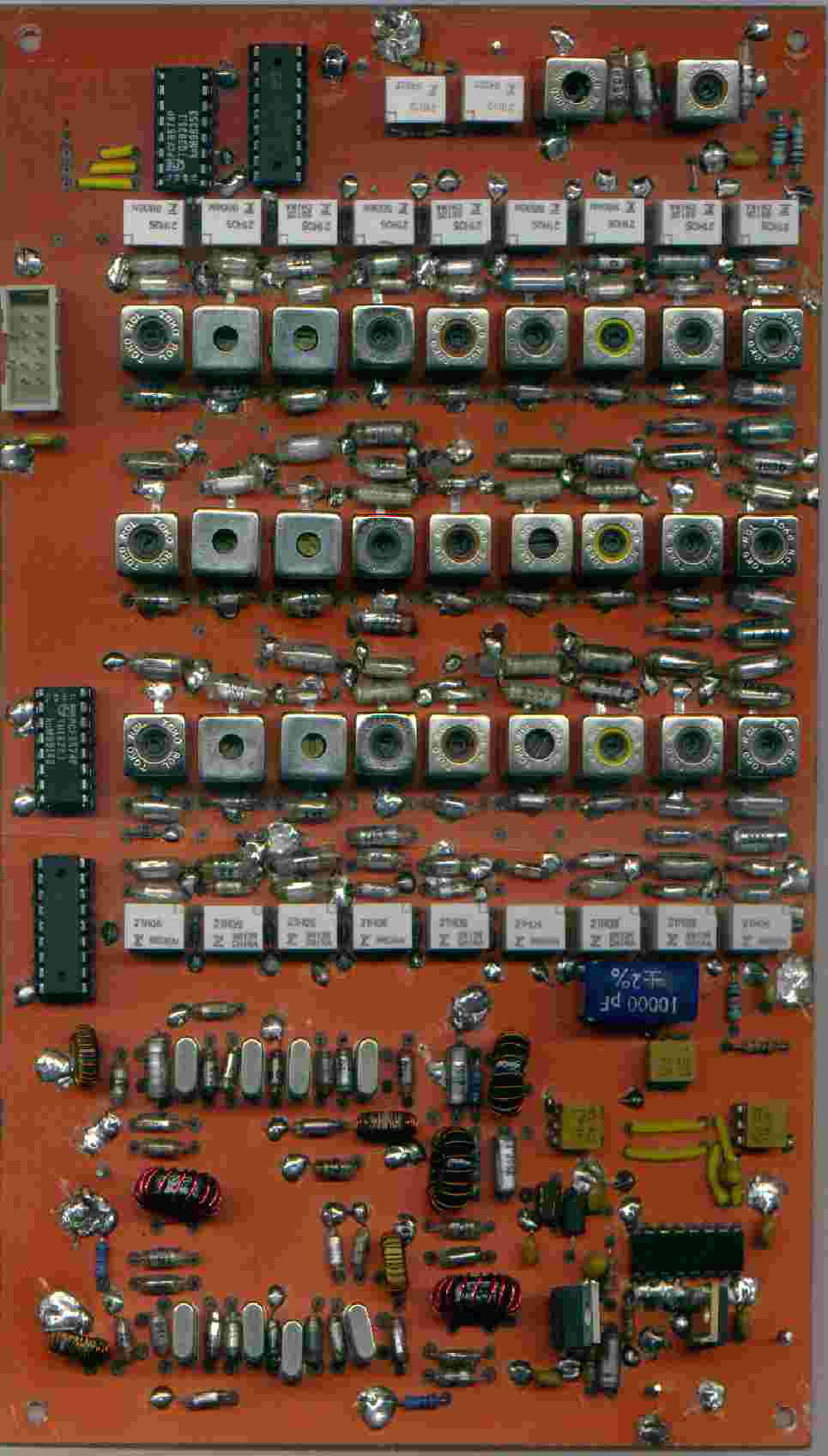
Picture 1 – Front End Board
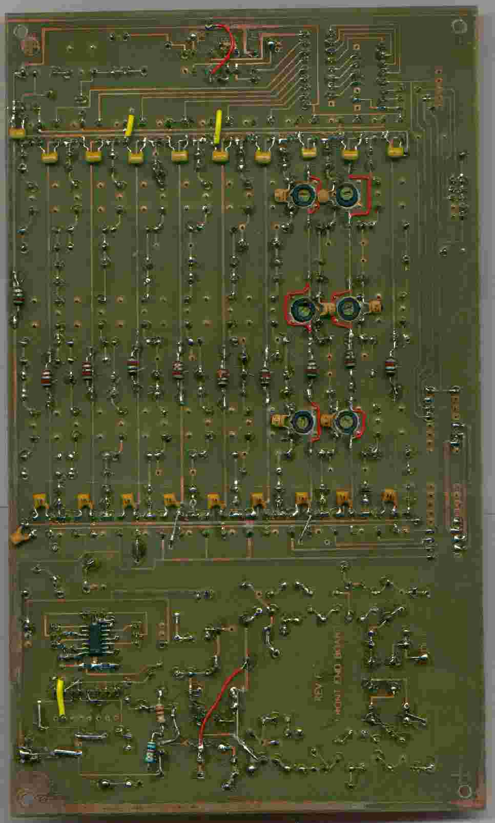
Picture 2 – bottom side of PCB
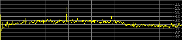
Picture 3 – Spectrum Lab display